Latest advance on seamless metal-semiconductor contact with


Atomic transistors based on seamless lateral metal-semiconductor junctions with a sub-1-nm transfer length

Unveiling the Future of Semiconductor Manufacturing: The Advanced Photolithography Aligner Explained

PDF) Transport properties and electronic phase transitions in two-dimensional tellurium at high pressure

Atomistic structures of various all-carbon contacts. a An AB-stacking
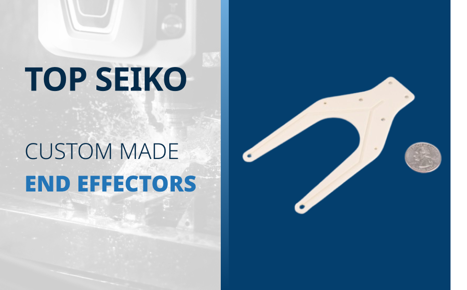
High-Performance Ceramic End Effectors - Top Seiko Co,. Ltd.

Alleviation of Schottky barrier heights at TMDs/metal interfaces with a tunneling layer of semiconducting InSe nanoflake - ScienceDirect
ELNES at the 1T /2H-MoTe 2 boundary. (a) A HAADF image showing the

Alleviation of Schottky barrier heights at TMDs/metal interfaces with a tunneling layer of semiconducting InSe nanoflake - ScienceDirect

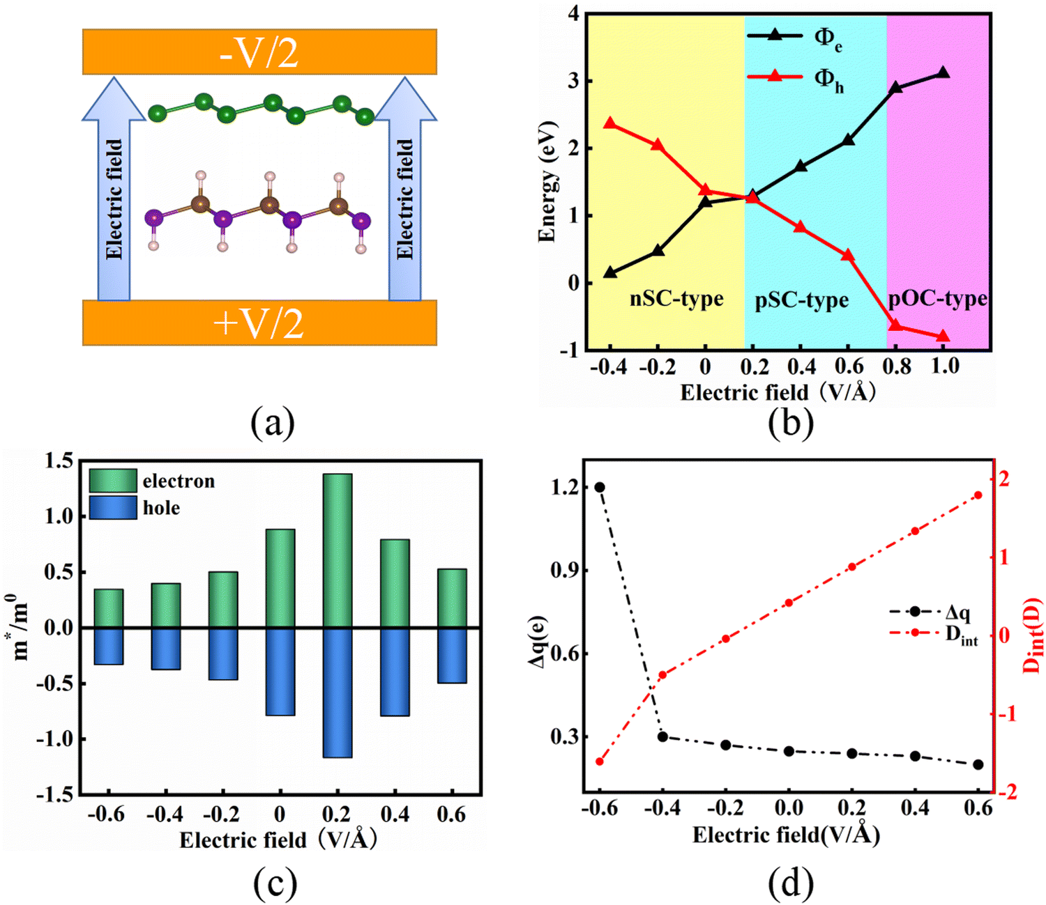
Latest advance on seamless metal-semiconductor contact with ultralow Schottky barrier in 2D-material-based devices - ScienceDirect
New way to render colors revolutionizes camera performance
Transition from Schottky to Ohmic contacts in 2D Ge/GaAs heterostructures with high tunneling probability - Physical Chemistry Chemical Physics (RSC Publishing) DOI:10.1039/D3CP06189B

Performance prediction of current-voltage characteristics of Schottky diodes at low temperatures using artificial intelligence - ScienceDirect
DMP Factory 500 Solution - Metal 3D Printer