Schematic illustration of GAB nanofabrication process. Top: fabrication

Schematic illustration of the fabrication process (a) of the soft PDMS

a) Schematic illustration of the fabrication of a hierarchical porous

Effective broadband electromagnetic wave absorption performance of

Nanoimprint lithography for high-throughput fabrication of metasurfaces

a and b) Schematic diagrams illustrating the fabrication of ordered

IMP and Nanotopochip platforms. (A) IMP fabrication process showing

Polymeric and biological membranes for organ-on-a-chip devices

Absolute values of the etch rate Ik 1 I obtained by linear fitting

SEM images of PDMS pillars. The pillars were fabricated by molding

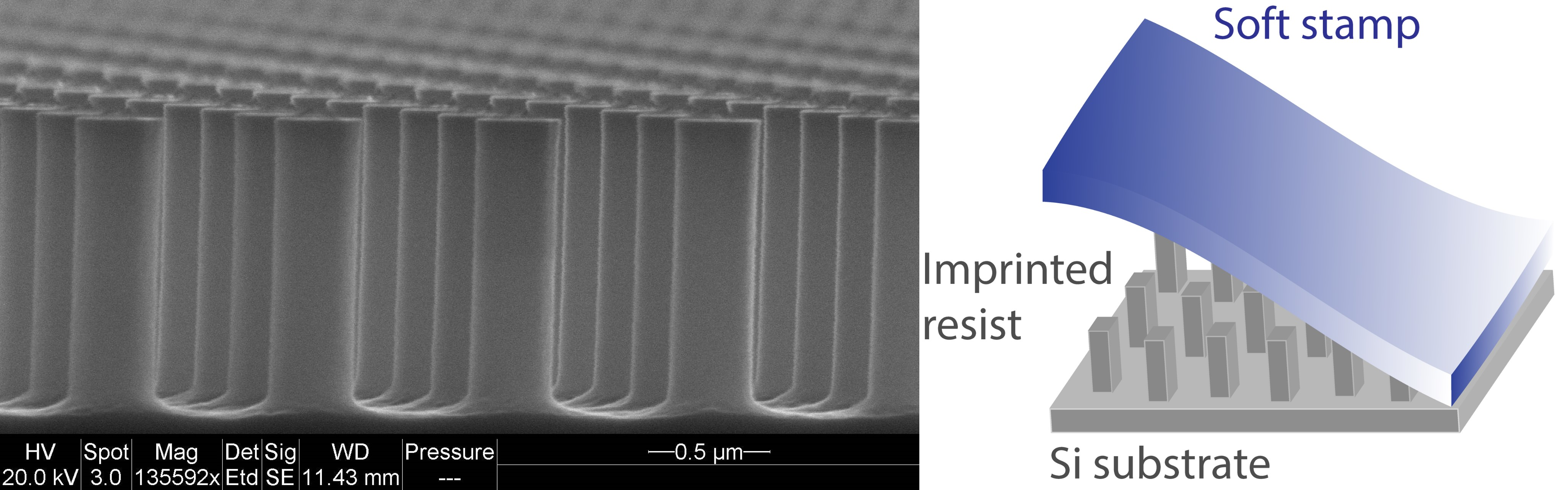
Schematic diagram of the UV curable nanoimprint lithography (UV
Nanomaterials, Free Full-Text