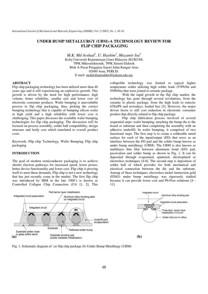
Figure 2 from Under Bump Metallurgy (UBM)-a technology review for

PDF) Under bump metallurgy (UBM) - A technology review for flip chip packaging

The failure mechanism of two stages dissolution of a 10- m-thick Cu
PDF) Pb-free Sn/3.5Ag wafer-bumping process and UBM (under bump metallurgy) study

Figure 2 from Under Bump Metallurgy (UBM)-a technology review for flip chip packaging
High Performance Electroless Nickel that's Lead and Cadmium-Free

Figure 1 from Effect of Under Bump Metallization (UBM) Quality on Long Term Reliability

The surface characteristics of under bump metallurgy (UBM) in electroless nickel immersion gold (ENIG) deposition - ScienceDirect

Materials, Free Full-Text

The surface characteristics of under bump metallurgy (UBM) in electroless nickel immersion gold (ENIG) deposition - ScienceDirect

PDF) Under Bump Metallurgy (UBM)-a technology review for flip chip packaging

PDF) Under bump metallurgy (UBM) - A technology review for flip chip packaging

61387 PDFs Review articles in SOLDERING

Effects of Under Bump Metallurgy (UBM) Materials on the Corrosion of Electroless Nickel Films

Micromachines, Free Full-Text