Multi-Layer PCB Stackup: .062 Finished Thickness

PCB stack-up of 8-layer test board

A schematic diagram of sodium aerosol sampling system installed in

a The effect of air jet velocity on the moisture content of paper

α Vs ρ, single-source Pareto traffic

PCB stack-up of 8-layer test board

How to Plan Multilayer PCB Stackup - RAYPCB

PCB stack-up of 8-layer test board

Targets are modeled as entering at locations p1, p2, …, p4 at the
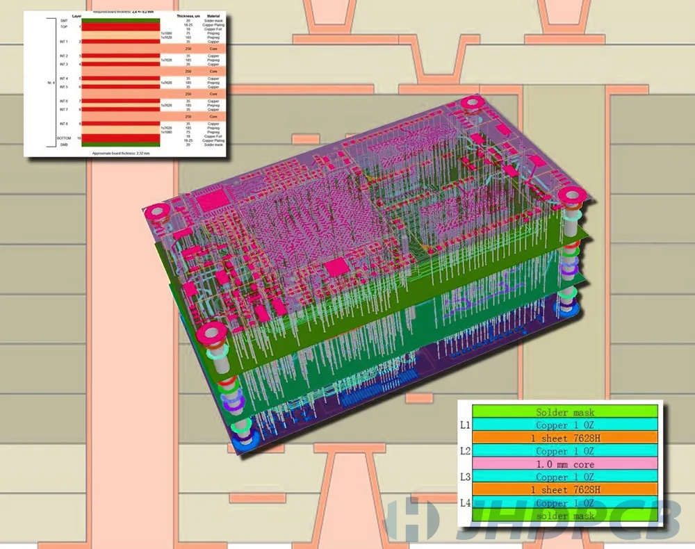
Design Rules, Structure And Variance Of PCB Stackup. - Jhdpcb

Analytical curve parameters and statistics for thiazolidinone PG15

Normalized shear modulus reduction of GF/EP cross-ply laminate
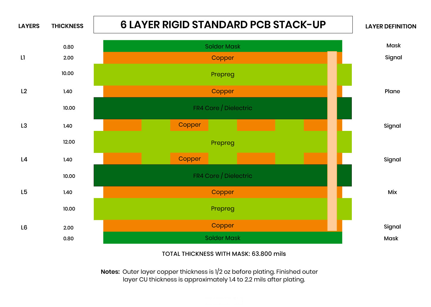
PCB Stack-Up Guide & Examples
Representative chromatogram of blank plasma (A), plasma spiked

Targets are modeled as entering at locations p1, p2, …, p4 at the