
Description
This case study focuses on the challenges and solutions that we implemented to design complex HDI boards with stacked vias.
How HDI Boards Can Be More Economical

How to allow microvia between two inner layers? - Layout - KiCad.info Forums
HDI PCB High Density Interconnect - Andwin Circuits
HDI PCB: Pushing the Limits of Your Electronics - MOKO Technology

HDI PCB Design,Manufacturing and its cost
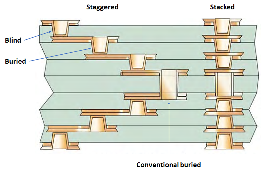
Case study: 8 and 14-layer HDI with Stacked Vias

Understanding Proper PCB Design (Part 2) - Circuit Cellar

High-Speed PCB Design- Layer Stack-Up, Material Selection, and Via Types
What's HDI? Design Basics and the HDI PCB Manufacturing Process
Related products


You may also like

Carnival in Brazil in 2025
)
Buy BUYONN Women Yellow Spandex Saree Shapewear (M) Online at Best Prices in India - JioMart.
Sudadera de French Terry para hombre Brasil

Soft Skills for Nurses eBook : Merchant, Sajid: : Kindle Store
Ivy yoga socks - SLENDDY

Fire TV Stick 4K (2023) Media Streamer with Alexa Voice Remote

Expedition Down Knickers Herre Fjällräven Isolerede bukser

DELIMIRA Women's Front Closure Bras Unlined Full Coverage Floral
Women CEP Ultralight No Show Socks – Calzuro Canada
$ 29.99USD
Score 4.7(609)
In stock
Continue to book
You may also like
Carnival in Brazil in 2025
Buy BUYONN Women Yellow Spandex Saree Shapewear (M) Online at Best Prices in India - JioMart.
Sudadera de French Terry para hombre Brasil
Soft Skills for Nurses eBook : Merchant, Sajid: : Kindle Store
Ivy yoga socks - SLENDDY
Fire TV Stick 4K (2023) Media Streamer with Alexa Voice Remote
Expedition Down Knickers Herre Fjällräven Isolerede bukser
DELIMIRA Women's Front Closure Bras Unlined Full Coverage Floral
Women CEP Ultralight No Show Socks – Calzuro Canada
$ 29.99USD
Score 4.7(609)
In stock
Continue to book
©2018-2024, followfire.info, Inc. or its affiliates